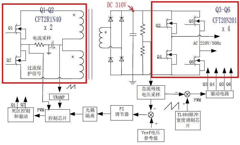
On the low-voltage side of the inverter, two medium and low voltage high current MOS transistors Q1 and Q2 (CFT2R1N40) (40V/150A) serve as power output tubes, transmitting energy to the primary of the step-up transformer. On the high-voltage side of the inverter, the secondary output of the step-up transformer is rectified and filtered to obtain a 310V DC voltage. Four high-voltage power transistors Q3-Q6 (CFT20N201) (200V/20A) convert 310V DC high voltage into AC 220V/50HZ AC voltage output.


